Goal
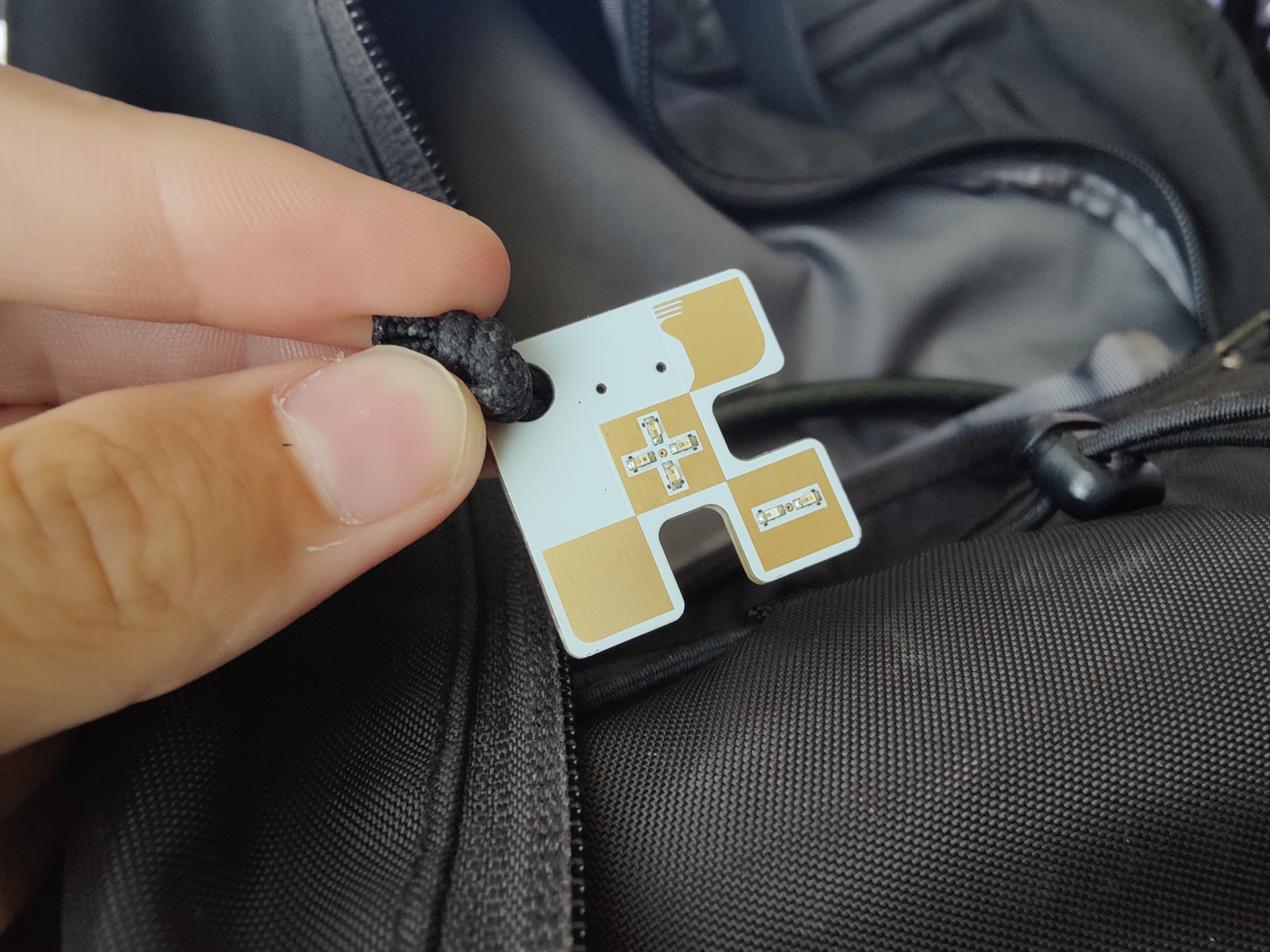
To make a keychain in the shape of the HyTech logo that can be connected to a USB-C power source and flash 6 LED lights on a 53% duty cycle. The circuit models the Ready-To-Move light used on the car to indicate that high voltage power is connected to the motors.
Background/Introduction
Starting this project, I had little experience with PCB design, reading datasheets, soldering, and none at all with Altium Designer. Throughout the project, I learned a lot about the process of designing PCBs, parsing datasheets, and using Altium, to the point where I can comfortably work with these tools and complete similar tasks on my own.
Designing LM555 Timer Component/Footprint
In order to make the keychain LEDs flash, I needed a timer component on the PCB. I opted to go with an LM555 Timer, since it can operate in astable mode and continuously oscillate between high and low outputs, with a very easily adjustable duty cycle (only requiring two resistors and two capacitors). Along with this, LM555s are widely available and inexpensive.
Starting the PCB design, I had to create a component in Altium to represent the LM555 timer in the schematic. This was fairly simple, and I only had to reference the pins on the datasheet for proper labelling.
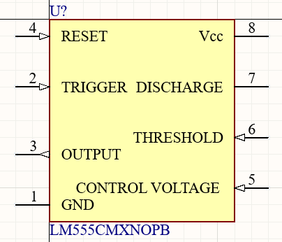
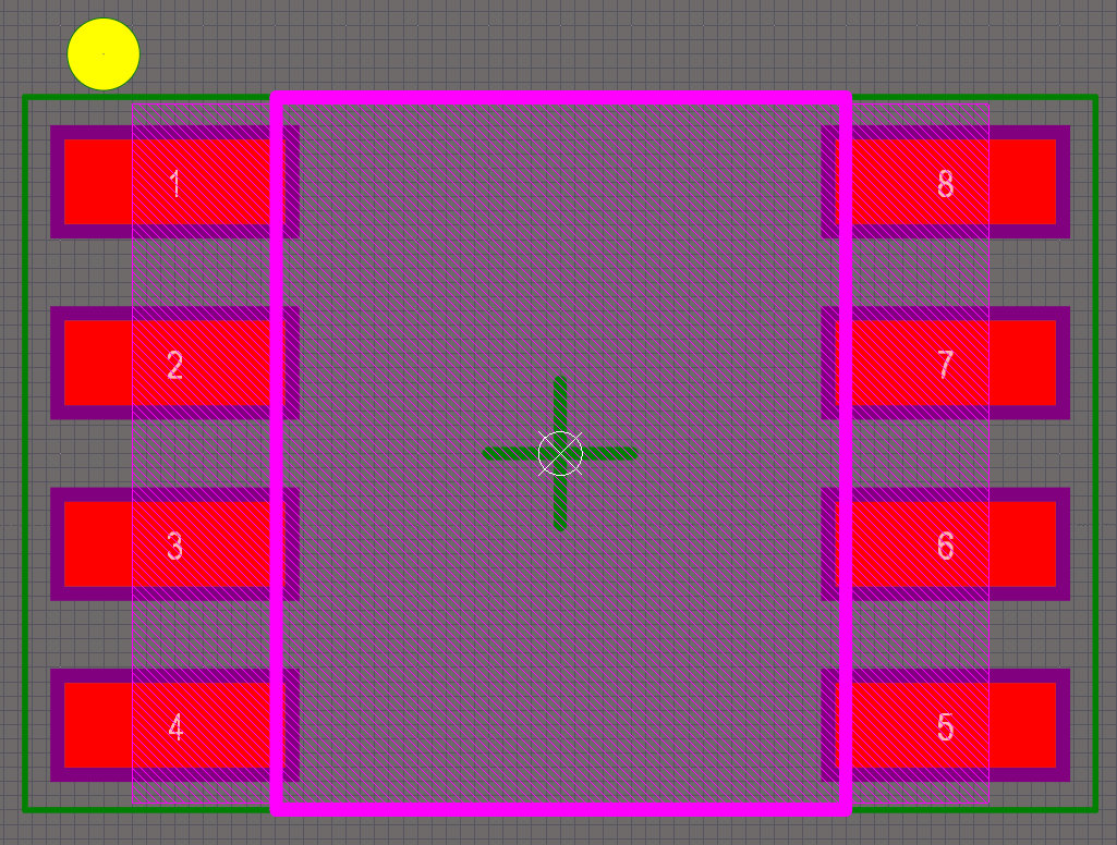
After this, I also has to create the component’s footprint, for eventually placing and routing the component in the actual design of the PCB. This was also a simple process, using a variety of measurements from the datasheet in order for the pads to properly match the component when soldering later on.
Designing Timer/LED and USB-C Port Schematics
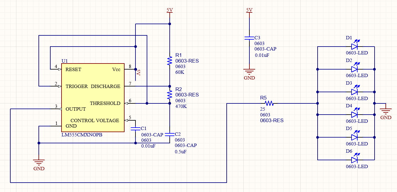
After creating the LM555 component, I created a schematic to depict the necessary connections for the LEDs to blink on a cycle the timer output. The overall design wasn’t very difficult, since the datasheet provided an example circuit that I could base my design on. Below, you can see that I connected a 5 volt power source to the timer component, and using the specific values I calculated for the resistors and capacitors referencing the datasheet, my design resulted in the timer outputting a high signal 53% of the time, with a frequency of 2.88 Hz. Combined with a decoupling capacitor to reduce voltage fluctations, the timer connects to the 6 LEDs, using a resistor to decrease the current supplied to each and prevent them from burning out.
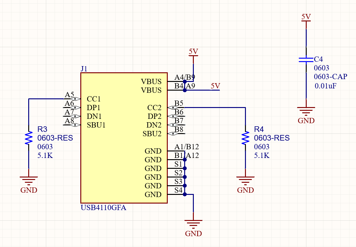
Next, I created the schematic for the USB-C port that would supply power to the keychain. The component itself already existed in the library I was using, so all I had to do was add a decoupling capacitor, output of 5V, ground connection, and most importantly, a specific pair of pull-down resistors on CC1 and CC2. From my research online, the combination of resistors depicted is commonly used to make a USB-C port draw 5V power from its source.
Creating PCB Shape/Design
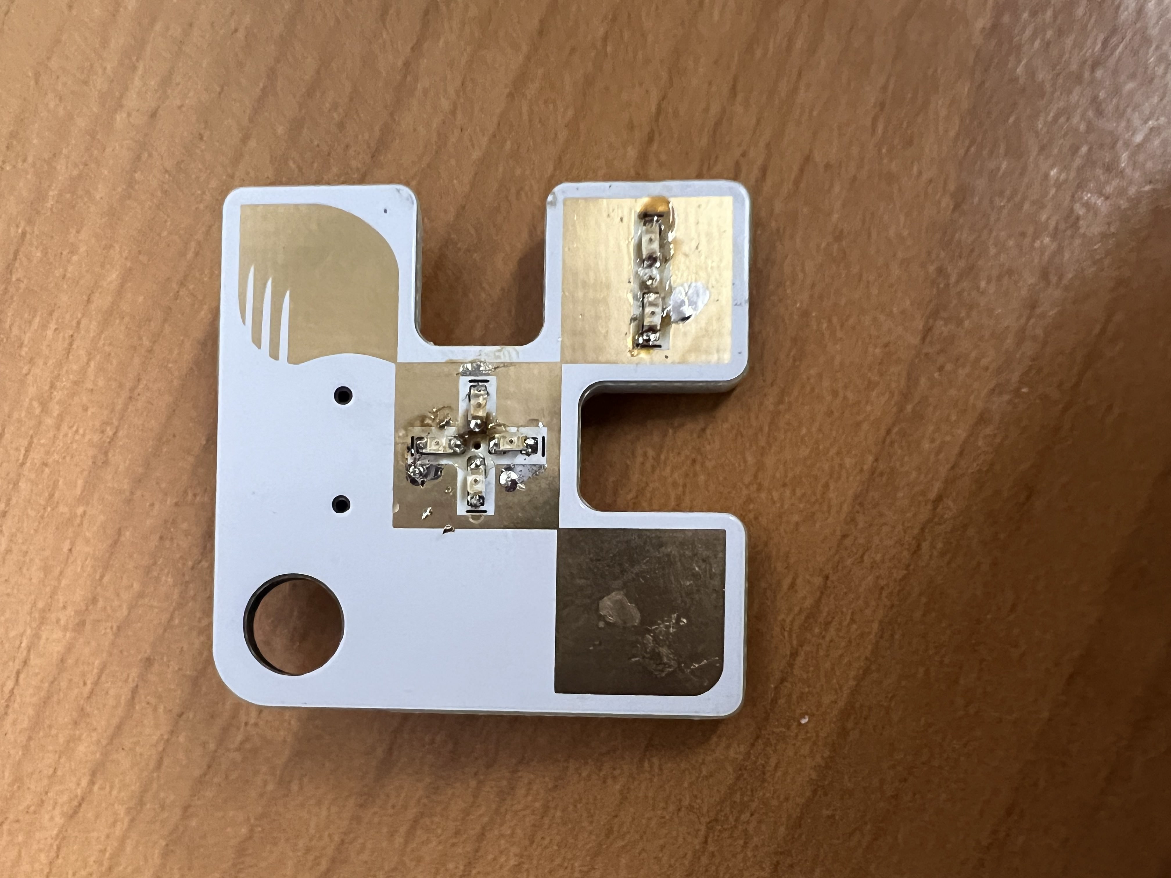
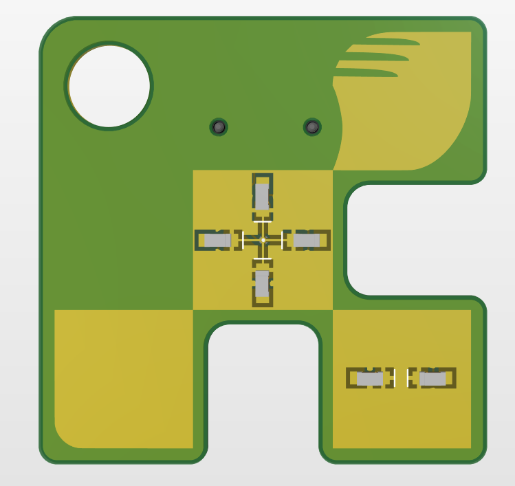
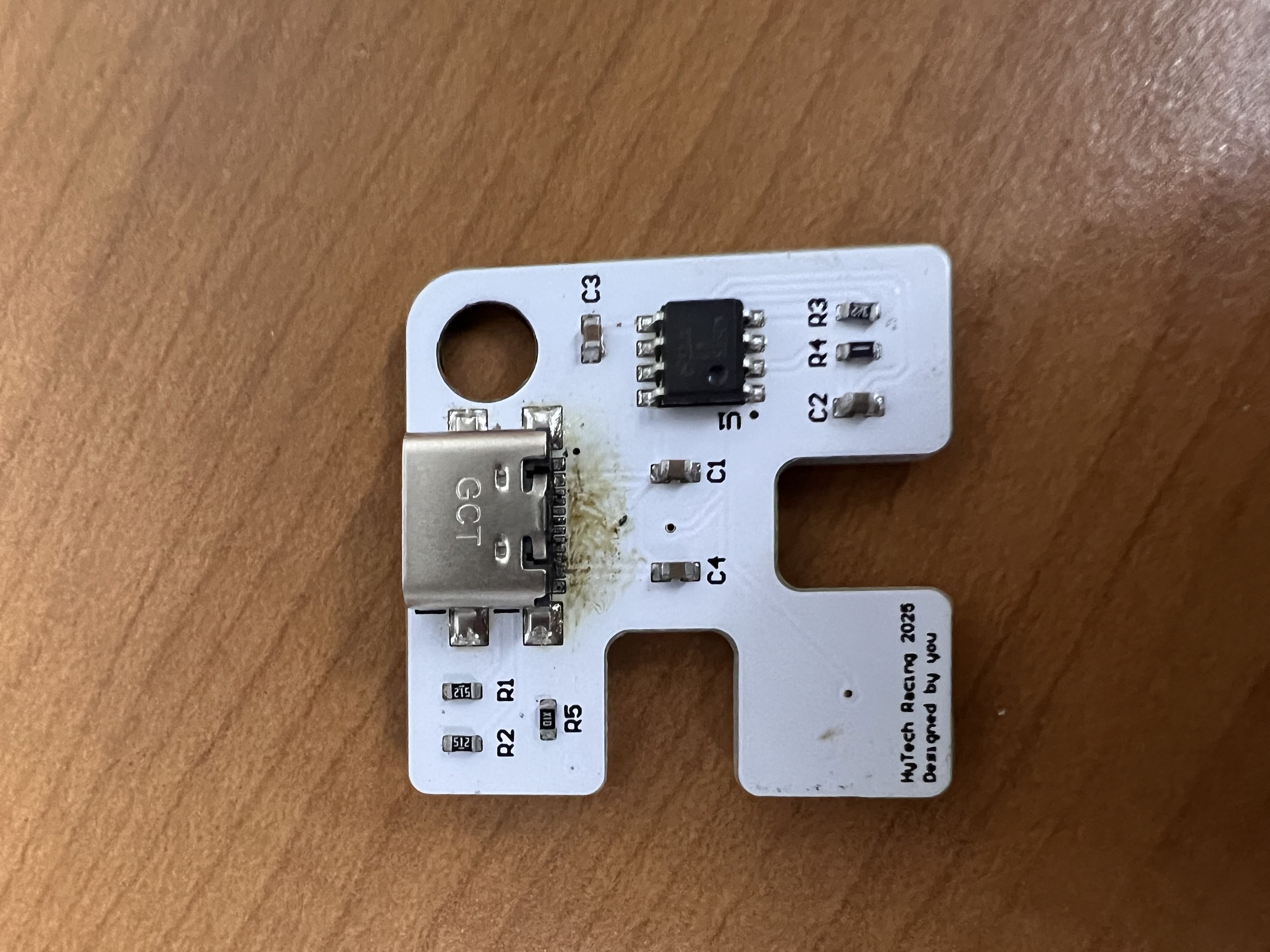
After designing the schematics, I needed the PCB shape to place them on. The PCB I designed was in the shape of the HyTech logo, with a hole in the corner to attach to a key ring or something similar. For the printed logo, I used holes in the solder mask, causing the gold-plated copper to show through.

Placing and Routing Components
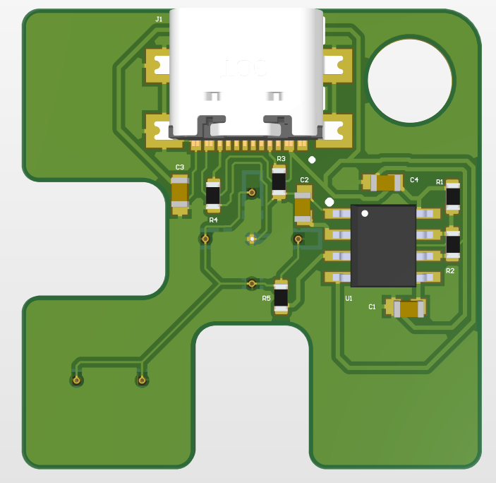
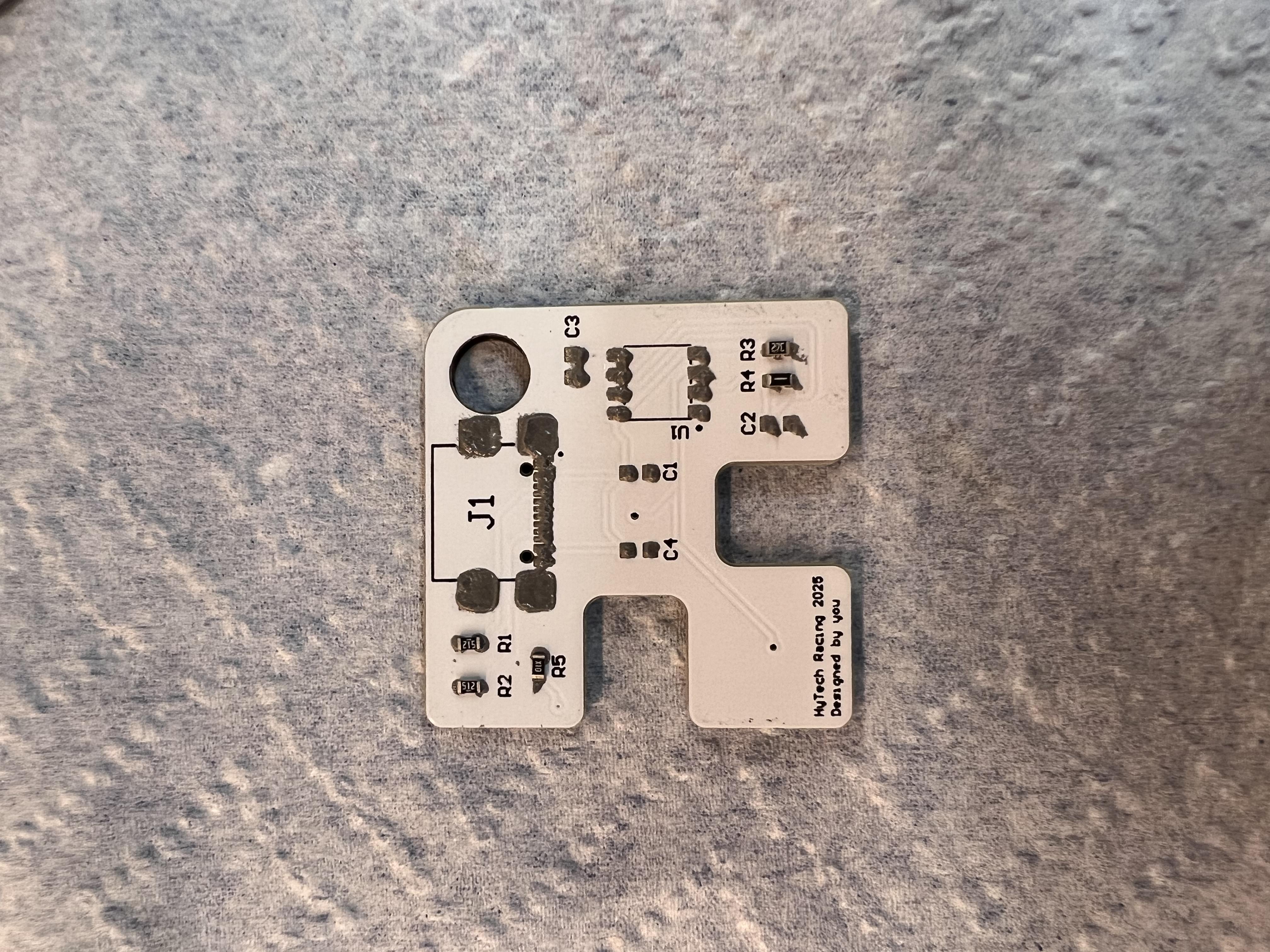
Finally, I had to place and route the schematics/components I had designed for my PCB. This included resistors, capacitors, LEDS, the USB C port, and the timer component. After placing the LEDs in a cross shaped pattern on the front, I placed the rest of the components on the back of the PCB in order to have as clean of a front to my keychain as possible. The biggest constraints I had as a result were the minimal usage of vias that went along with this, making it very difficult to connect everything on the back and the front without overlapping, and the lack of space for traces on the back, due to the large number of components squeezed into one place. However, after many trials and errors, I was able to arrange my components in a way that allowed me to route traces between all the components my schematics detailed as needing connections. However, in the future, I could definitely arrange my components more efficiently. If I were to remake this project or redesign it in the future, I would reroute the PCB to use fewer traces and connect them without going under the USB-C port or taking any unneccessarily long paths.
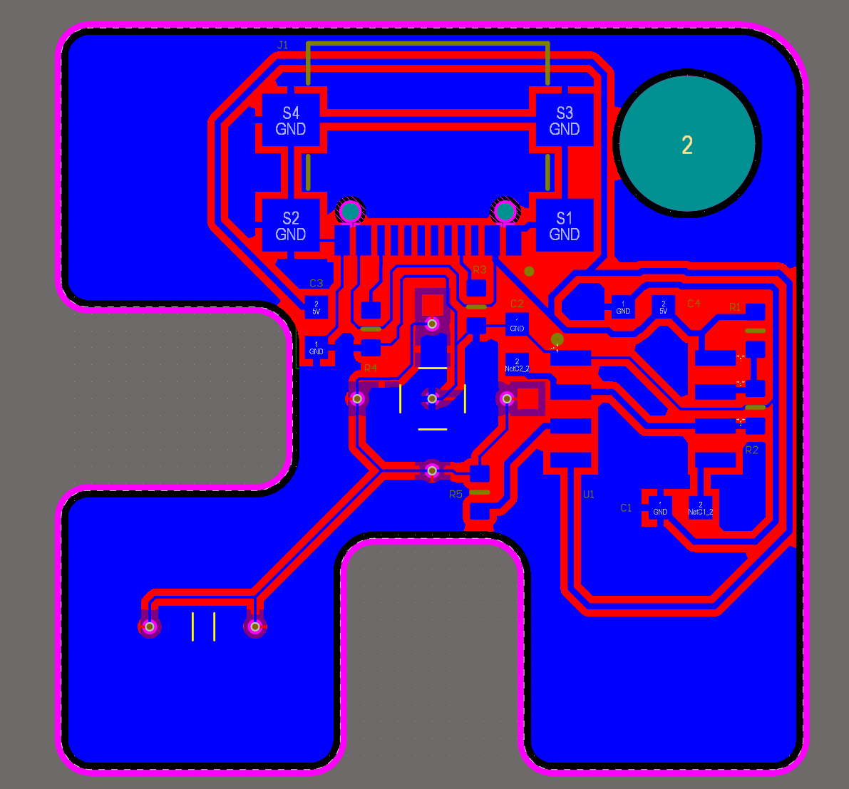
Below, you can see the 3d model in Altium of the back and front of the PCB I designed. This design passed all the design rule checks implemented in altium, signifying that it was ready to be manufactured.
Soldering the Final PCB
Finally, the design was sent to a manufacturer. Since the PCB I designed used many tiny components designed for surface mount soldering, I received the PCB and a stencil for spreading the solder paste.
For the first step in actually soldering the board, I used the stencil to spread a thin layer of solder paste over each pad. However, when taking the stencil off, my finger slipped and I ended up slightly smearing the paste. This would later cause bridging between some of the pads, but I could clean this up afterwards. Afterwards, I simply had to place the components onto the solder paste using tweezers.
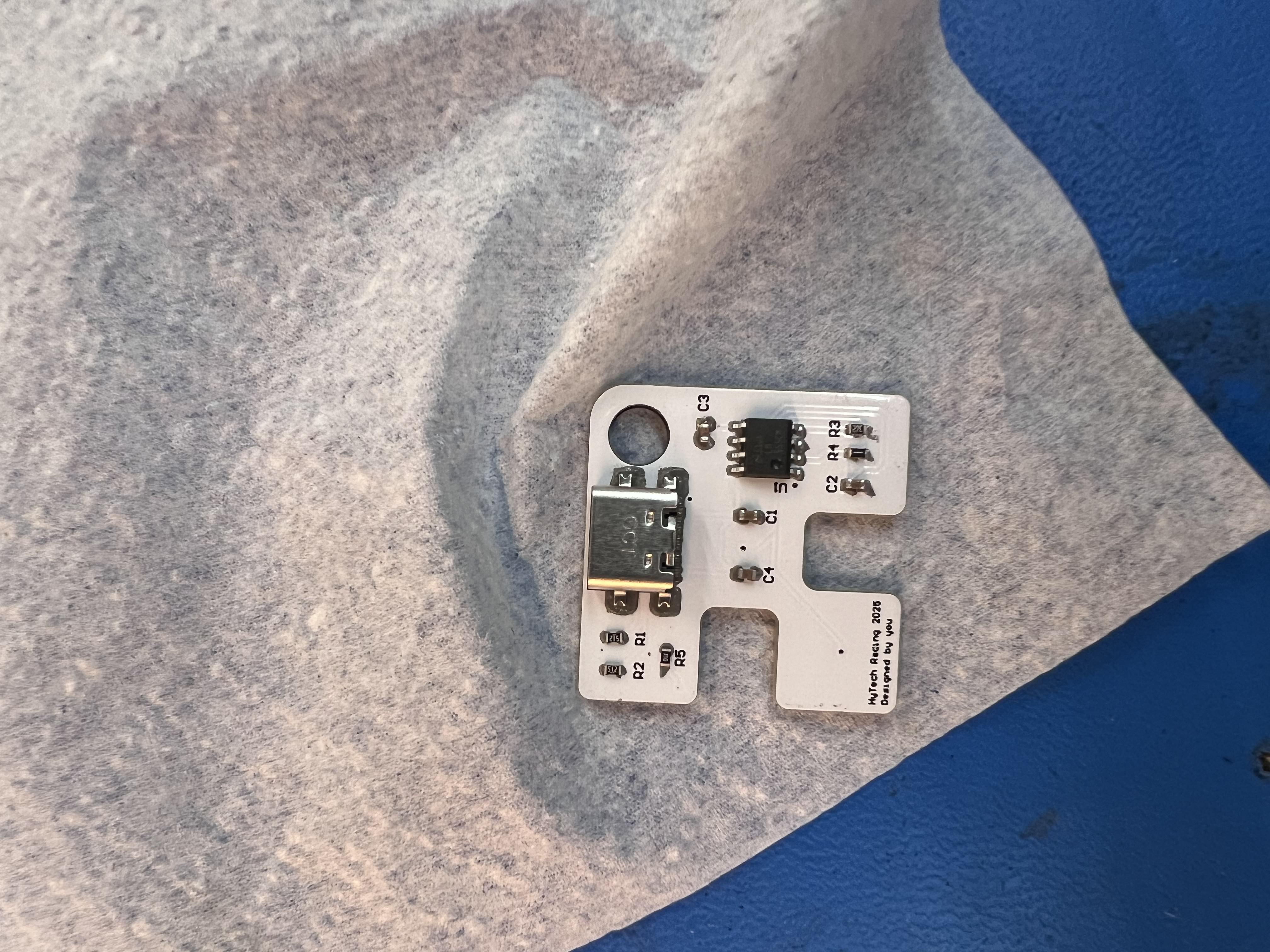
Next, I placed the PCB inside a reflow oven to melt the solder, so that when it was cooled afterwards, the components would be soldered to the board.
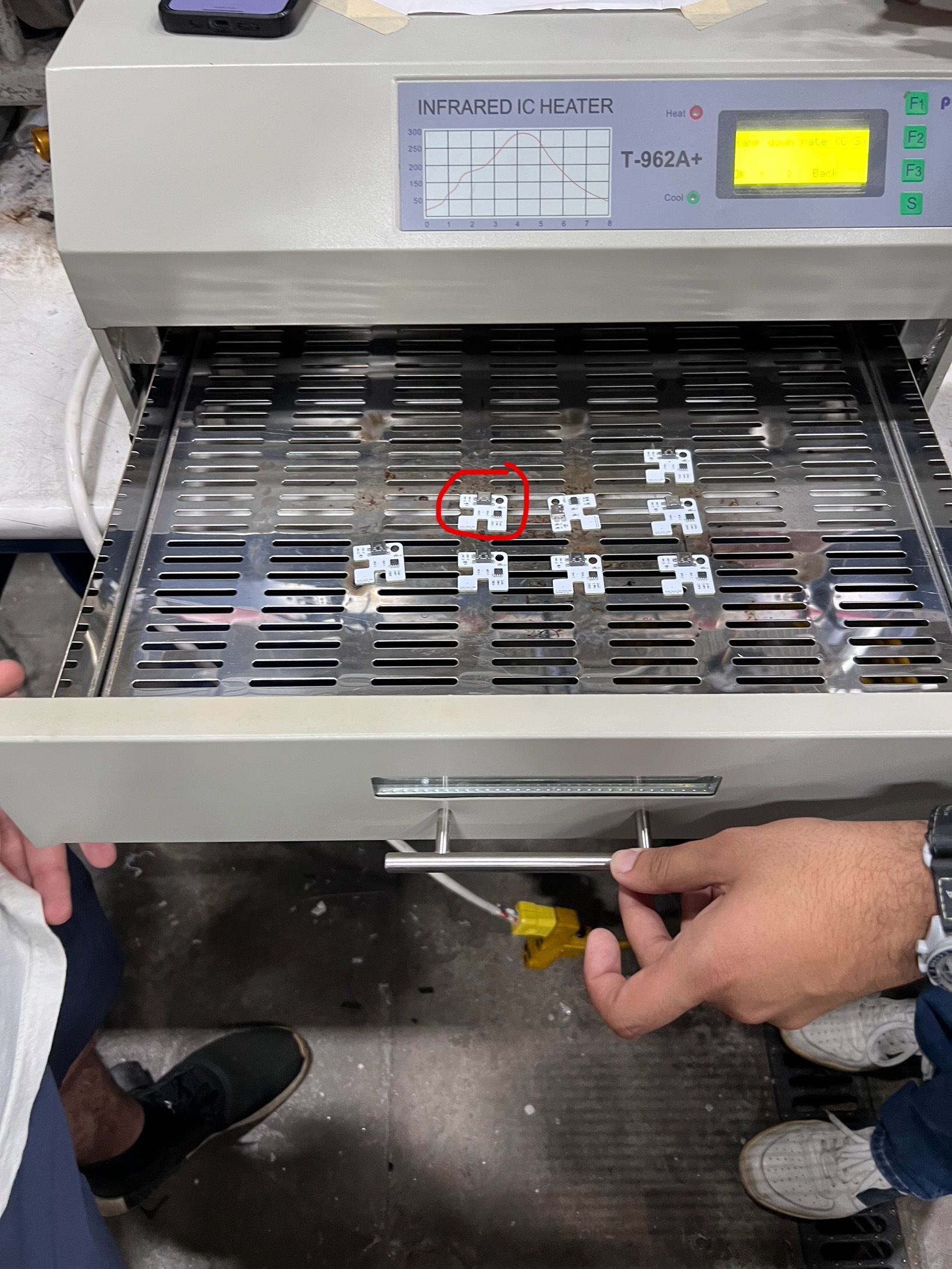
As expected, my board had bridging between a few of the pads connecting the USB-C port. I was able to fix this though by using desoldering wick and reheating the solder using a soldering iron.
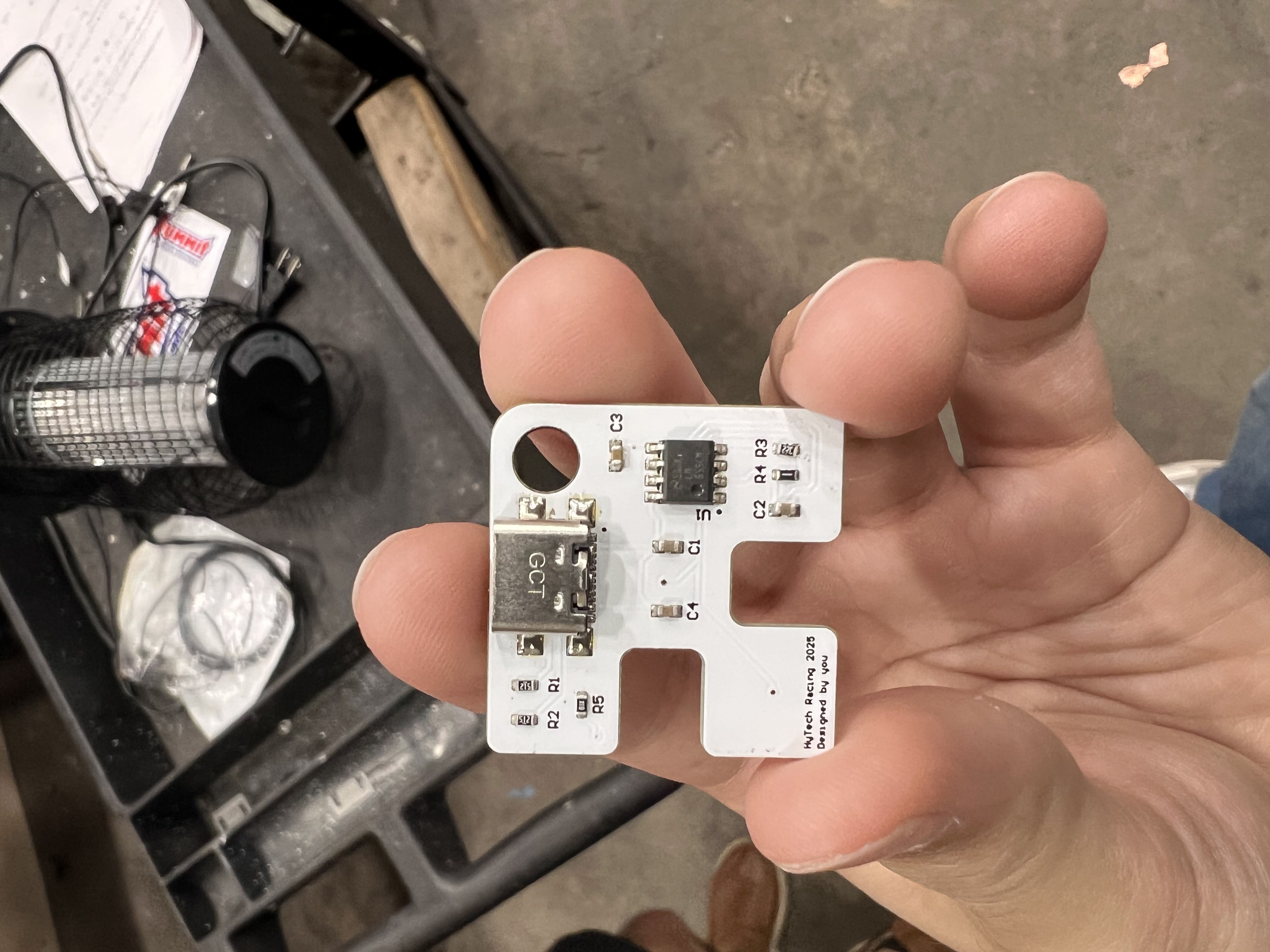
Finally, I only had the LEDs on the front left to solder. For this part, I soldered the components by hand using a soldering iron. After this step, I plugged the board into a standard USB-C cable connected to a laptop and the LEDs flashed as expected.